Semiconductor Metrology / Production Equipment
XRF / EDX / WDX
Product Description
- XRF / EDX / WDX
- Wafer Thin Film Metal Thickness & Composition Measurement
- Handheld XRF
- EDX Elemental Analysis, Jewelry, RoHs, WEEE applications
- Wavelength Dispersive XRF (WDX)


AAS / ICP
Product Description
- AAS / ICP
- Sequential Inductively Coupled Plasma Spectrometer (ICP)


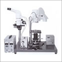
SEM
Product Description
- The visual system of Scanning Electron Microscope
- Surface analysis


Wafer Thickness / Film Stress
Product Description
- Wafer Film Stress / Film Thickness Measurement
- Low-k / Cu Material Stress Hysteresis / Thermal Desorption Measurement
- Sheet Resistivity, Rs / Leakage for Ultra-Shallow Junction Measurement
- Thin Wafer Thickness / Roughness / Warp / Bump Height Measurement
- 4-Point Bend Environmental Low-k Adhesion Tester
- Surface 3D Video Microscope and Surface Profiler instrument


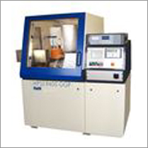
Wafer Grinding
Product Description
- Wafer Grinding, Thinning & Polishing Machine
- Ultra-Thin Wafer Thinning Machine
- Wafer Edge Grinding Machine

Wafer UV Curing / Mounter / Cleaning
Product Description
- Vacuum Wafer Mounter Machine
- Wafer UV Curing Machine
- Wafer Cleaning Machine

Spin Coater / Etcher / Mask Aligner
Product Description
- Spin Coater / Spin Etcher / Developer / Spin Cleaner
- Mask Aligner / Mask Cleaner / Plasma Cleaner
- Lift off system

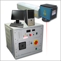
Laser Marking / Cutting
Product Description
- Laser marking on wafer
- Laser cutting / marking system for sheet metal, plastic, leather, wood